The Advantages of Press Fit PCB Technology
Press fit PCB technology is revolutionizing the electronics industry with its unique approach to establishing connections between printed circuit boards (PCBs) and electronic components. Unlike traditional soldering methods, which involve applying heat and solder to create connections, press fit technology utilizes mechanical force to achieve a reliable and gas-tight connection. Let's explore the advantages of press fit PCB technology and its significance in modern electronics.
Elimination of Soldering Process: One of the primary advantages of press fit PCB technology is the elimination of the soldering process. This eliminates the need for high-temperature soldering, reducing thermal stress on the PCB and components. It also eliminates the risk of solder-related defects such as cold joints, solder bridges, and solder cracks. By removing soldering from the assembly process, press fit technology simplifies manufacturing and increases production efficiency.
Increased Reliability: Press fit connections provide a robust and reliable electrical connection. The mechanical force applied during assembly ensures a gas-tight connection, resulting in excellent electrical conductivity and signal integrity. The absence of solder also eliminates the risk of solder degradation over time due to factors like temperature variations, vibrations, and thermal cycling. As a result, press fit PCB technology offers enhanced long-term reliability and stability in electronic systems.
Enhanced Serviceability and Repairability: Press fit technology allows for easy removal and replacement of components without the need for desoldering. This makes repairs and component upgrades faster and more convenient, reducing downtime and maintenance costs. The press fit contacts can be easily inserted or extracted using specialized tools, simplifying the rework process and minimizing the risk of damage to the PCB or surrounding components.
Compatibility with Various PCB Materials: Press fit PCB technology is compatible with a wide range of PCB materials, including FR-4, high-temperature substrates, and flexible PCBs. This versatility makes it suitable for diverse applications across different industries. Additionally, press fit connectors can be used for both single-sided and multi-layer PCBs, allowing for flexible design options and scalability.
Suitable for High-Density Applications: Press fit technology enables high-density PCB designs by eliminating the need for large solder joints. The press fit contacts occupy minimal space on the PCB, allowing for closer component placement and increased routing density. This is particularly advantageous in applications where space is limited, such as mobile devices, aerospace systems, and automotive electronics.
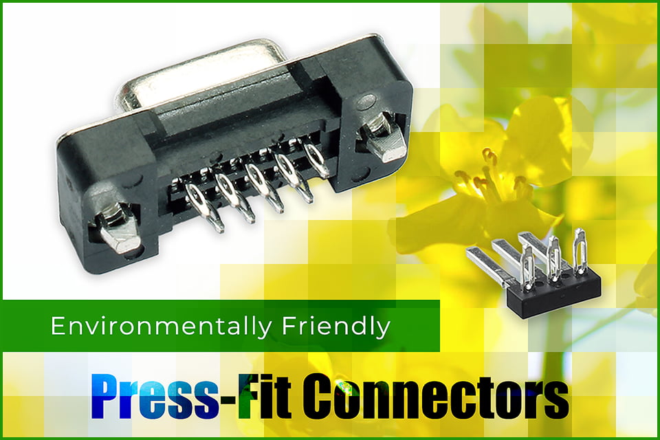
Environmentally Friendly: As press fit PCB technology does not involve the use of solder, it eliminates the need for lead-based solders, which are harmful to the environment. This aligns with the global push for more environmentally friendly manufacturing processes and the reduction of hazardous substances in electronic products.
As the electronics industry continues to evolve, press fit PCB technology provides a reliable and efficient solution for connecting PCBs and components, facilitating the development of innovative and high-performance electronic devices.
Elimination of Soldering Process: One of the primary advantages of press fit PCB technology is the elimination of the soldering process. This eliminates the need for high-temperature soldering, reducing thermal stress on the PCB and components. It also eliminates the risk of solder-related defects such as cold joints, solder bridges, and solder cracks. By removing soldering from the assembly process, press fit technology simplifies manufacturing and increases production efficiency.
Increased Reliability: Press fit connections provide a robust and reliable electrical connection. The mechanical force applied during assembly ensures a gas-tight connection, resulting in excellent electrical conductivity and signal integrity. The absence of solder also eliminates the risk of solder degradation over time due to factors like temperature variations, vibrations, and thermal cycling. As a result, press fit PCB technology offers enhanced long-term reliability and stability in electronic systems.
Enhanced Serviceability and Repairability: Press fit technology allows for easy removal and replacement of components without the need for desoldering. This makes repairs and component upgrades faster and more convenient, reducing downtime and maintenance costs. The press fit contacts can be easily inserted or extracted using specialized tools, simplifying the rework process and minimizing the risk of damage to the PCB or surrounding components.
Compatibility with Various PCB Materials: Press fit PCB technology is compatible with a wide range of PCB materials, including FR-4, high-temperature substrates, and flexible PCBs. This versatility makes it suitable for diverse applications across different industries. Additionally, press fit connectors can be used for both single-sided and multi-layer PCBs, allowing for flexible design options and scalability.
Suitable for High-Density Applications: Press fit technology enables high-density PCB designs by eliminating the need for large solder joints. The press fit contacts occupy minimal space on the PCB, allowing for closer component placement and increased routing density. This is particularly advantageous in applications where space is limited, such as mobile devices, aerospace systems, and automotive electronics.
Environmentally Friendly: As press fit PCB technology does not involve the use of solder, it eliminates the need for lead-based solders, which are harmful to the environment. This aligns with the global push for more environmentally friendly manufacturing processes and the reduction of hazardous substances in electronic products.
As the electronics industry continues to evolve, press fit PCB technology provides a reliable and efficient solution for connecting PCBs and components, facilitating the development of innovative and high-performance electronic devices.